
Reverse Engineering a PCB: What the Board Still Tells You
Sooner or later a product outlives its documentation. The engineer who designed it leaves, the company that built it closes, a drive fails, and what is left is the hardware.
The hardware is still the primary source. A board carries its own record of what it is — the layers it was built from, the parts fitted to it, the connections between them, the reference designators printed on its surface, and, sometimes, the names the original designer gave to its nets.
Recovering that record and turning it back into data a fabricator and an assembly house can build from is what PCB reverse engineering does.
This article is about how that work is actually done: what a board can tell you, what it cannot, and where the limits sit.
Why a Board Gets Reverse-Engineered
The reasons are usually mundane rather than dramatic.
- The product still sells, and the original manufacturer no longer supports it.
- The design files exist somewhere, but nobody can find them or nobody can open them.
- A contract manufacturer has the Gerber files but not the source design behind them.
- A company is being acquired, and the buyer is getting hardware instead of a design.
- The board works, and rewriting it from scratch would mean re-testing everything that already works.
This is a different job from preparing an existing design for production. That work starts from complete files and asks whether they are consistent and buildable, which is what a production readiness review does. Reverse engineering starts from the hardware, because there are no files to review yet.
One thing is worth stating before anything else, because it shapes the whole project. What comes out of reverse engineering is not the original design. It is a new set of design data that produces the same board, and it will not be the same file the original engineer worked from.
The work also has a precondition. It applies to boards you own or are authorized to work on, and that boundary decides whether a project can start at all.
What the Board Still Carries
A finished board gives you five kinds of information, and they are not equally reliable.
Silkscreen. Reference designators — R12, C47, U3 — are the board's index. Without them, a netlist is a list of coordinates. If the designer also printed net names, the silkscreen is more than an index: the nets arrive already named, and a trace you have not followed yet already tells you what it is for. Not every design does this. When one does, it removes a large part of the guesswork.
Component markings. Value codes, polarity bands, package sizes, manufacturer marks, date codes. Enough to identify most passives and many ICs, and enough to mislead you, because marking codes are short and not unique across manufacturers.
Copper. Trace geometry, trace widths, via positions, pours and their boundaries.
Mechanical data. Board outline, hole positions and diameters, connector footprints, mounting hardware, board thickness.
The parts themselves. What is fitted, what is left unpopulated, and what has been reworked.
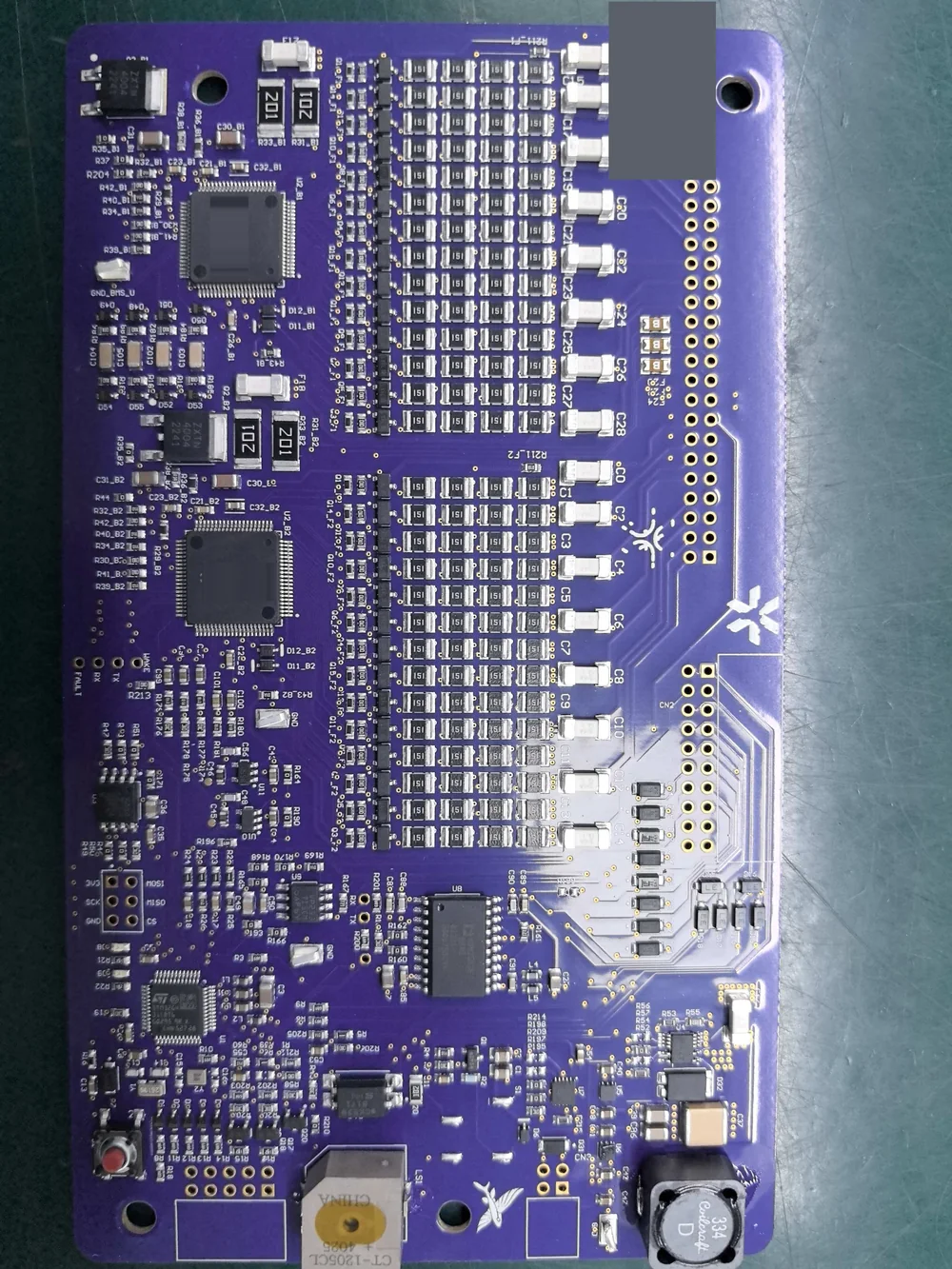
The list of what the board does not carry is shorter and matters more.
A board does not record its stackup — the dielectric thicknesses and copper weights behind the outer layers. It does not record impedance targets, because a finished board shows what a trace is, not what it was designed to be. It does not carry the tolerance, voltage rating or temperature coefficient of a part whose marking has worn off. A board records what was built. Nothing on it records why.
The Layers You Cannot See
On a two-layer board, everything in the design sits on a surface you can photograph. On a four-layer board, half the copper is inside the laminate, and that is where the clean answers stop.
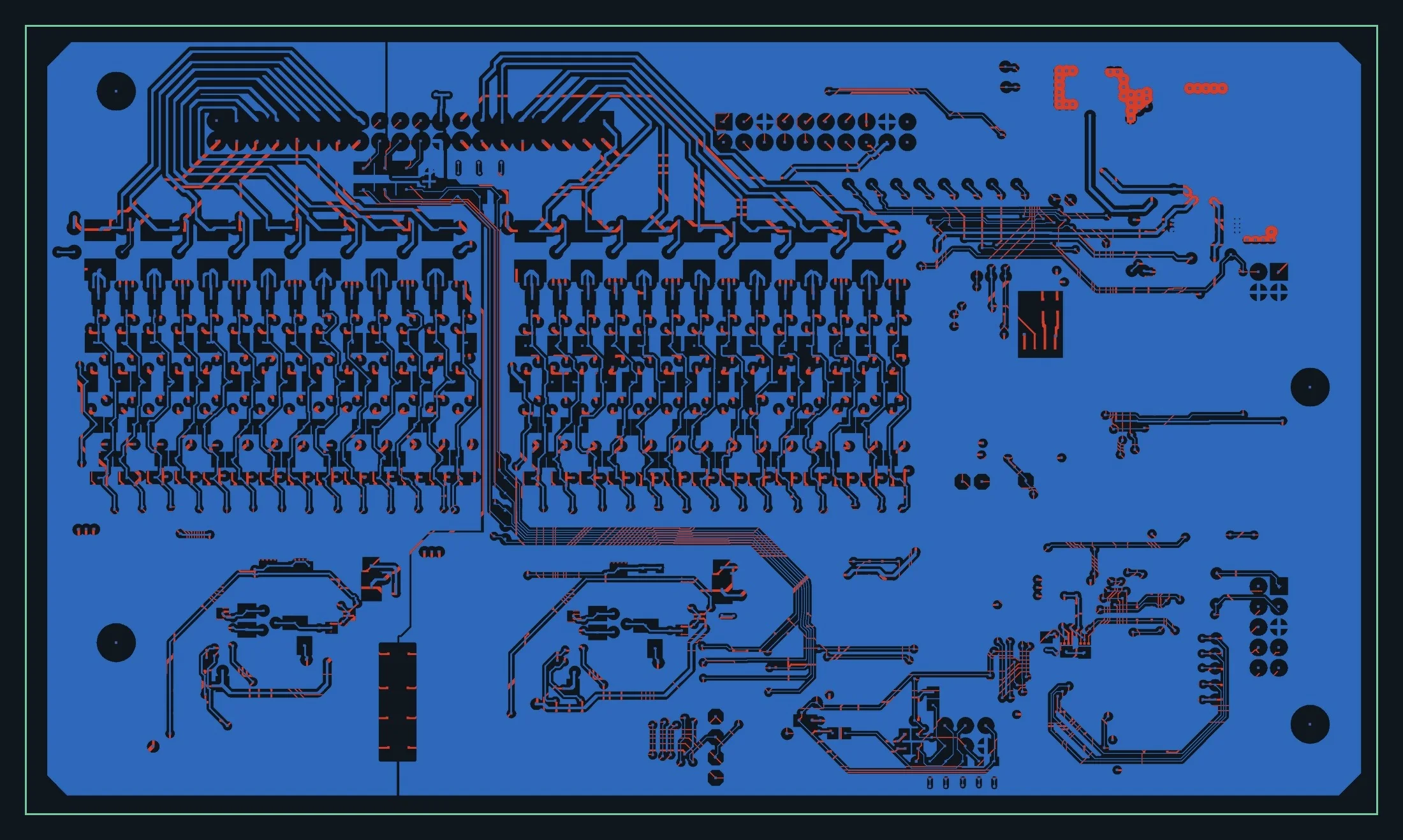
There are five ways to deal with an inner layer, and each one costs something.
X-ray imaging. Non-destructive. One view through the board, so the copper of every layer in the beam path lands on the same image. It establishes that a feature is there and roughly where it sits — a via that lands where you expect, a plane that extends under a region — but no layer is separated from the ones above and below it, and reading a net out of the stack is interpretation rather than measurement.
X-ray CT. Also non-destructive, and different in kind rather than in degree: the board is imaged from many angles and the data is reconstructed into a volume, so an inner layer can be looked at without the layers around it. What that resolves depends on the scanner, the resolution it can reach, the layer count and copper weights of the board, and how the scan is set up — thin inner traces are the hard case, and what comes out is an image to trace from, not a layer file.
Cross-sectioning. A destructive cut through the board, viewed on edge under a microscope. What it shows is the construction rather than the circuit: dielectric thickness, copper weight, the plating inside a hole barrel, and where a trace on one layer meets the trace on the next. It is a slice through the board, not a view of it, so it says nothing about routing.
Layer separation, or delamination. The other destructive route, and the one that does produce artwork. Taking the layers apart opens the inner copper into plan view, so an inner layer can be imaged directly instead of inferred — routing, pours and clearances together. It also leaves a board that no longer works, which means anything still to be measured had to be measured first, and the board had to be one you could afford to lose.
Inference. Power and ground planes are usually most of the inner copper, and their extent can often be established from the vias that land on them and the outer-layer routing that reaches those vias. Signal routing buried on an inner layer can be inferred the same way. Inference is not evidence.
Whichever route is taken, an inner layer that was inferred has to be handled differently from a layer that was photographed. It should be marked as inferred in the data, and it should be the first thing checked when the rebuilt boards arrive. Written into a CAD file without that distinction, it is indistinguishable from a layer that was read directly off the board — and by the time anyone finds out, the boards exist.
Tracing Connectivity
Tracing is where most of the time goes. The output is a netlist: which pins connect to which, and through what.
The starting points are whatever is already labelled — connectors, IC pins, test points, and any net names on the silkscreen. From there the work alternates between visual tracing under magnification and continuity measurement with a meter, moving between the two as the board allows.
Two mistakes account for most of the errors.
A trace followed visually that does not connect where it appears to. It passes under a component, or changes layer at a via and continues somewhere else. This is what the meter is for.
A connection that is real but is not a net. A meter reads continuity through a 0 Ω resistor, through an inductor, through a ferrite bead, and through a diode if the polarity happens to suit it. Reading continuity is a measurement. It does not tell you that the two pins are on the same net.
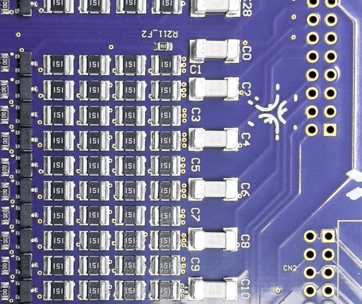
A board that repeats the same circuit many times changes the economics of tracing, because one instance can be traced carefully and the others verified against it. The board in these photographs is a battery management board, and it does exactly that: the same channel block appears again and again, and the reference designators carry the instance, so the same position in a different channel is the same designator with a different suffix.
The structure helps, and it is easy to over-trust. The channel block repeats; the way each channel connects back into the rest of the board does not, and those per-instance connections have to be traced one at a time — which is exactly what a shortcut would skip.
Identifying Components and Rebuilding the BOM
A bill of materials is a purchasing document. What is on the board and what has to be bought are usually the same list, and the exceptions are where this part of the work gets difficult.
A bill of materials has a fixed set of columns, and the board fills them with varying confidence. One line covers every designator that shares the same part, and the quantity on that line is the count of those designators. A single line can therefore stand for a handful of positions or for a hundred. Here is the shape of one. Part numbers and manufacturers are blanked out in this example — those two columns name one specific maker's part, and on a customer's board they are not ours to publish.
| Designator | Part Number | Description | Footprint | Manufacturer | Qty |
|---|---|---|---|---|---|
| C4, C5, C6, C10, C11 | — | ceramic capacitor, 0.1 µF | 0603 | — | 5 |
| R64_F1, R64_F2, R65_F1, R65_F2 | — | thick-film resistor, 150 Ω | 1210 | — | 4 |
| R30_B1, R30_B2, R41_B1, R41_B2 | — | thick-film resistor, 100 kΩ | 0603 | — | 4 |
| D34_F1, D34_F2, D35_F1, D35_F2 | — | zener diode | SMA | — | 4 |
| Q3_F1, Q3_F2, Q4_F1, Q4_F2 | — | N-channel MOSFET | SOT-23 | — | 4 |
| U2_B1, U2_B2 | — | battery monitor and protection IC | TQFP-80 | — | 2 |
| U3 | — | SPI NOR flash, 32 Mb | SOP-8 | — | 1 |
| U8 | — | isolated transceiver | SOIC-20 | — | 1 |
Parts fall into three groups.
Marked. The value or the part number is printed on the part and can be read, sometimes only under magnification.
Coded. The marking is a short manufacturer code. It can usually be resolved, but codes are short and reuse across manufacturers is common, so the same three characters can mean different parts depending on the package and the maker.
Unmarked. Nothing readable. The package and the position in the circuit may narrow it down. They do not establish a part number, and a part number is what purchasing needs.
Then there is the part of a bill of materials that the board cannot supply at all. Capacitance can be measured; dielectric cannot. Resistance can be measured; tolerance and temperature coefficient cannot. A diode's polarity can be seen; its voltage and current ratings cannot. A board that works tells you a part was adequate. It does not tell you the margin that was designed in.
So rebuilding a bill of materials is design work, line by line. Every line where the board is silent is a choice, and it is the same kind of choice the original engineer made, with less information to make it from.
Rebuilding the Layout
The deliverable that matters most is the layout: a CAD database whose output reproduces the board.
It is worth being precise about what is and is not on the critical path. If the goal is to build this board again, what a fabricator and an assembly house consume is the layer artwork, the drill data, the board outline, the bill of materials and the placement data. A schematic is none of those. A schematic is a document written for people — the clearest possible statement of what the design is trying to do — and it is not required to make the board.
That makes the scope a real decision rather than a shortcut, and both answers are defensible.
Layout only. Faster and cheaper, and enough to rebuild the board as it is. What you give up is the readable statement of intent: later changes have to start from the netlist instead of a diagram, there is no schematic to run an electrical rules check against, and an engineer who inherits the project inherits geometry rather than reasoning.
Layout and schematic. Recovers the document as well as the data. It is a second piece of work with its own cost, and it is worth doing when the design is going to be changed — a component substitution, a respin, a cost reduction — rather than only rebuilt.
In the project shown here, the scope was the layout and the manufacturing data. No schematic was recovered, and that limitation is worth stating rather than glossing over, because it is the one that shows up later.
Below that decision sits a large amount of unglamorous work. Copper geometry has to be redrawn into a CAD database, and every layer checked against the physical board: pad sizes, clearances, annular rings, drill diameters, solder mask openings, silkscreen positions, and the registration of vias between layers.
Two of those layers deserve more attention than they usually get. Solder mask openings and drill data are the two whose errors surface last. A mask opening that is slightly too small still works, until a particular part with a particular tolerance is used. A drill that is slightly undersized still fits, until the part is a press fit or the connector is a tight one.
The stackup is the other gap. The board tells you its finished thickness and its layer count. It does not tell you the dielectric thicknesses or the copper weights behind them, and a fabricator needs those numbers if anything on the board is impedance-controlled. If nothing is, the gap does not matter much. If something is, the missing numbers have to be recovered another way, or re-specified deliberately.
Generating Fabrication and Assembly Data
Once the layout is rebuilt, the output is the same set of files any board design produces.
- One artwork file for each copper layer
- Solder mask, top and bottom
- Silkscreen, top and bottom
- Drill data, with plated and non-plated holes separated
- The board outline
- The bill of materials, at one agreed revision
- Placement data for assembly — position, rotation and side — with reference designators matching the silkscreen
A few entries in that list go wrong in predictable ways.
The whole dataset is defined from a single viewing direction, which means bottom-side layers are drawn mirrored relative to how they appear on the finished board. Get that convention wrong and the board comes back with its bottom silkscreen reversed. It is harmless electrically, because silkscreen carries no electrical function, but it is not the kind of error anyone wants to find on a production panel.
Placement rotation is the other one. Rotation is measured from a zero that different CAD tools and different assembly machines disagree about, and a systematic 90° error puts every part on the board sideways. It is caught by the first assembled unit, and only if somebody is looking at the board rather than at the test results.
Silkscreen also has to be regenerated rather than copied. Reference designators on rebuilt data have to land where the assembly house and any future repair technician expects to find them, which means checking them against the physical board rather than trusting the reconstruction.
What Comes Back
The first boards built from reconstructed data are the test of the reconstruction, and the useful comparison is physical rather than functional: does this board match the one it was reconstructed from.
A board that works shows that the data produces a working board. Whether the data matches the original is a separate question, because a reconstruction can be wrong in ways that do not stop it from working — a pad slightly larger, a mask opening slightly wider, an equivalent part substituted for one that is no longer available. Those are the differences that show up later, in yield or in a repair, rather than on the bench.
Where that comparison is made, it is made against the original board: artwork over artwork on a light table or in an overlay, hole for hole, with the registration between layers checked as closely as the layers themselves. Anything the reconstruction could not establish directly from the board — an inferred inner layer, a part substituted for one that could not be sourced — is flagged, and it is the first thing to check. Not every reconstruction gets the full comparison, and where it does not, the flags in the data are what the next engineer has to work from.
The analysis, the tracing, the layout and the fabrication data are produced by our product development team. Fabrication and assembly run through the established manufacturing partners we work with in China. That comparison is what closes the loop between the two.
What Reverse Engineering Does Not Give You
Three limits are worth stating plainly, because they are the ones that cause disappointment later.
It does not give you the original design. It gives you data that builds the same board. What does not carry across is the reasoning: a layout decision that was made for a reason becomes the geometry that came out of it.
It does not give you the firmware. A board and its software are separate problems, and recovering one tells you nothing about the other.
It does not cover everything on the board equally. The parts that were readable, the nets that were traced and the layers that were seen are recovered with confidence. The inner layers that were inferred, the parts with no marking and the connections that were assumed are recovered with less, and that difference matters most to whoever works on the board next. A reconstruction that presents all of it as equally solid is more dangerous than one that says which is which.
The boundary that stays fixed through all of it: this work applies to boards you own or are authorized to work on.
If the next step is changing the design rather than rebuilding it, that is a different piece of work — electronic product redesign starts from the netlist this one produces.
Ready to start your electronics project?
Send your files — or just a rough idea. We'll review your project and tell you the next step.
No files ready yet? That's fine — start the conversation and we'll tell you what's needed.